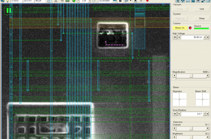
Circuit Edit involves the modification of existing ICs or electronic chips using focused ion beam technique. For example after tape out of the chip it can occur that the device does not function as it should. In that case, the designer can modify the circuit’s design and produce a new chip. This is a very expensive and time-consuming job (at least a few months). It is justified to spend a few $1000 to verify this re-design first. This means an adjustment is done to the physical chip. Subsequently it is investigated whether this has the desired result.
A circuit edit can be for example the removal of a functional block of circuit that is using too much power. Or we can make a connection so that a given signal is shorted. An edit can be for example the removal of a material such as the cutting of a metal track, but also the deposition of a conductive material so that a new electrical connection is realized. Not forget to mention we are talking about very small dimensions. Cutting traces of 200 nm is no exception. The figure below shows a cross section of a completed cicuit edit on a real chip. Two metal traces are connected to each other at points a and b. This type of connections are
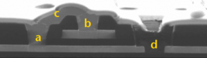
Cross section view of a performed circuit edit
also mentioned as vias. Next, both of these vias are connected by a strap c. This local connection consists of a metal deposition; often this is platinum or tungsten, but it can also be another material such as molybdenum. In the figure also a cut is shown at location d. After cutting the line the hole is filled with TEOS deposition which is insulating. A circuit edit job can contain multiple of these actions. A designer should always consider to have as less edits possible on one device. This because each single step is carrying risk of damaging the device. There is not much needed to destroy a sub- micron structure.
Nwells are exposed at the backside of the chip
Beside circuit edit we also use FIB to apply FIB probe- or bond pads. This to create and connect it randomly to signals on the chip. We are capable to deposit metals straps while insitu measure the resistance. This application can be very useful during Failure Analysis of a chip for fabless semiconductor companies or IDMs.