Get to know more about our services
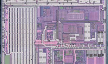
Competitor Analysis
Know your competitor! For strategic planning it is crucial to obtain technology intelligence to identify opportunities and threats.…
Read more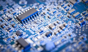
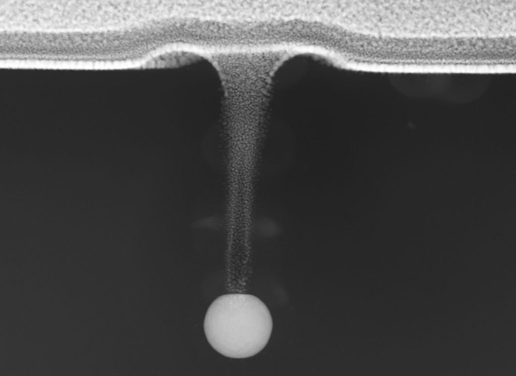
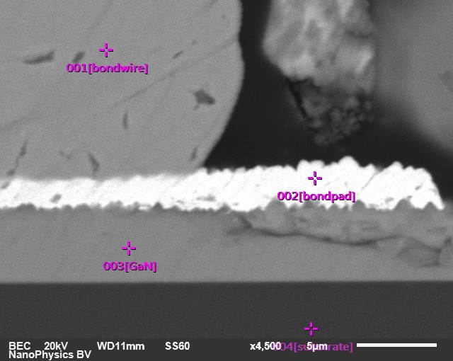
Failure Analysis Service
Failure analysis (FA) is the process of determining how or why a part has failed. This is often performed…
Read more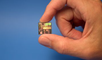
Patent Infringements analysis
For innovative high-tech companies it is crucial to defend your business. NanoPhysics B.V. can help to reveal detailed…
Read more
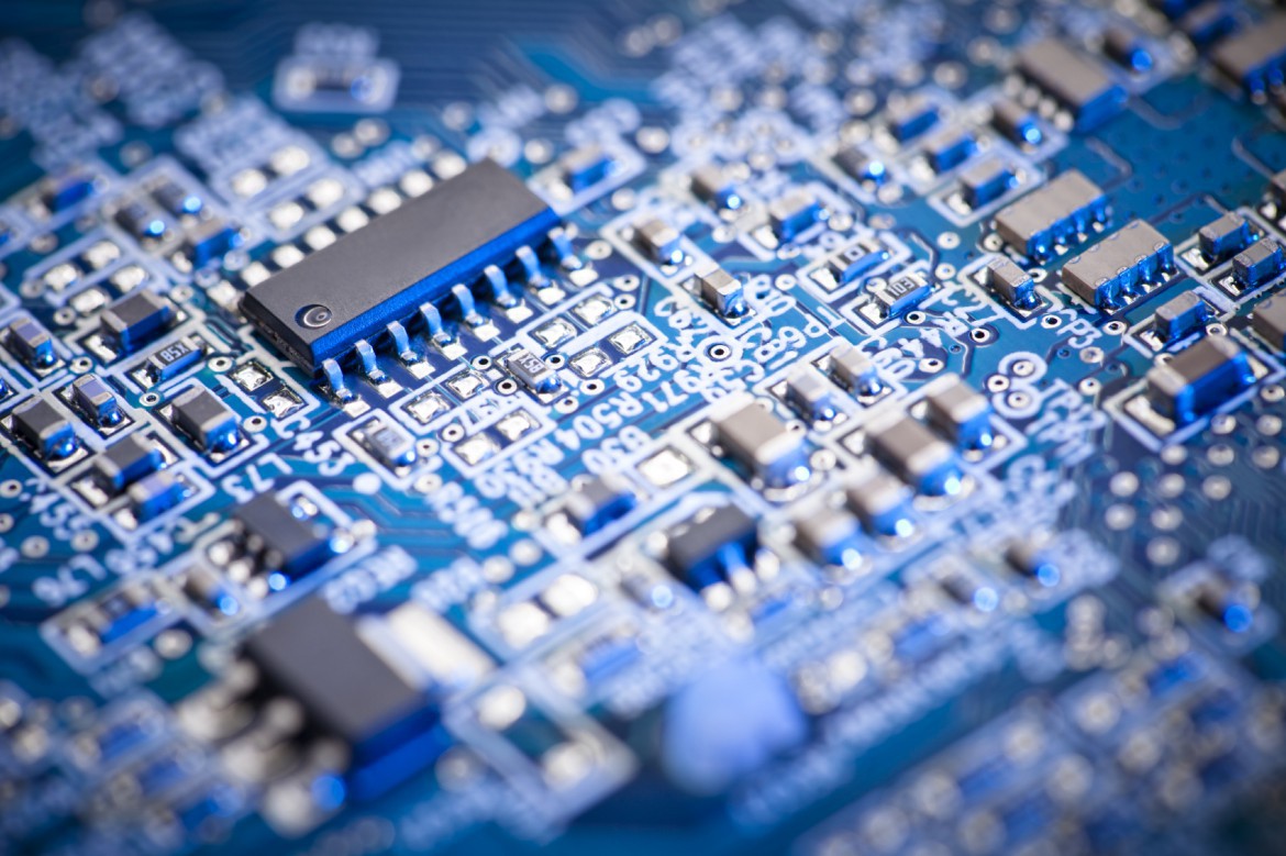
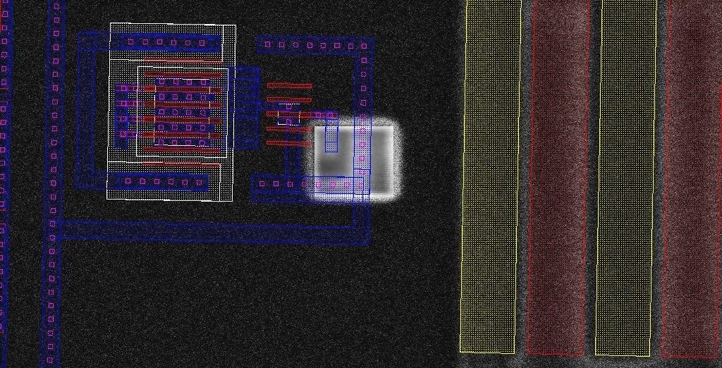
Circuit Edit
One of the FIB services NanoPhysics has to offer is circuit edit, which is a powerful technique to enhance the development…
Read more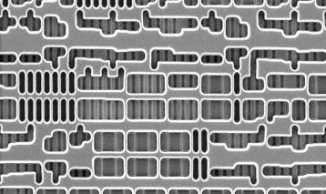
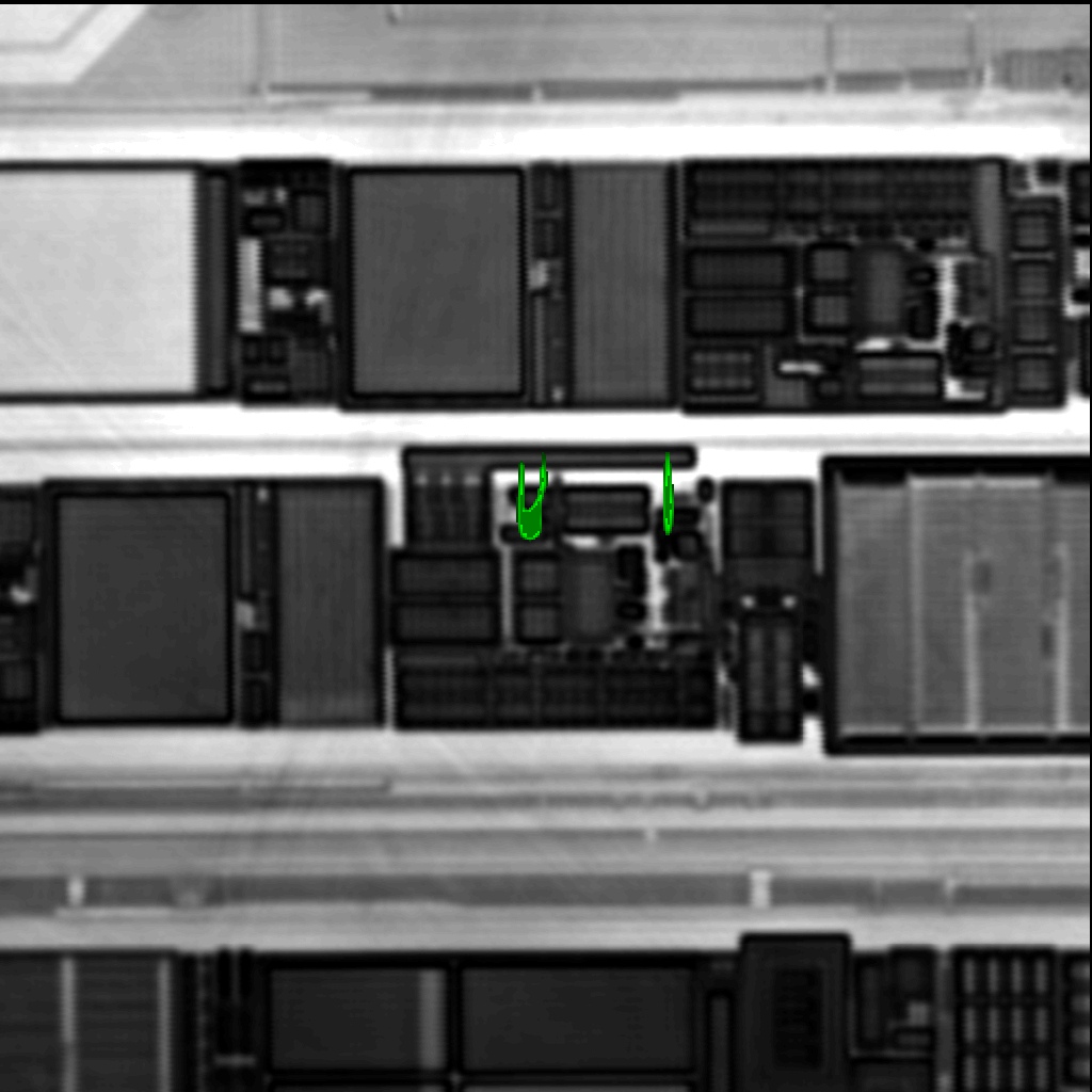
Chip Deprocessing
Chip Deprocesing Quite often the next step after Fault Localization like OBIRCH or Photon Emission is Destructive Physical Analysis…
Read more
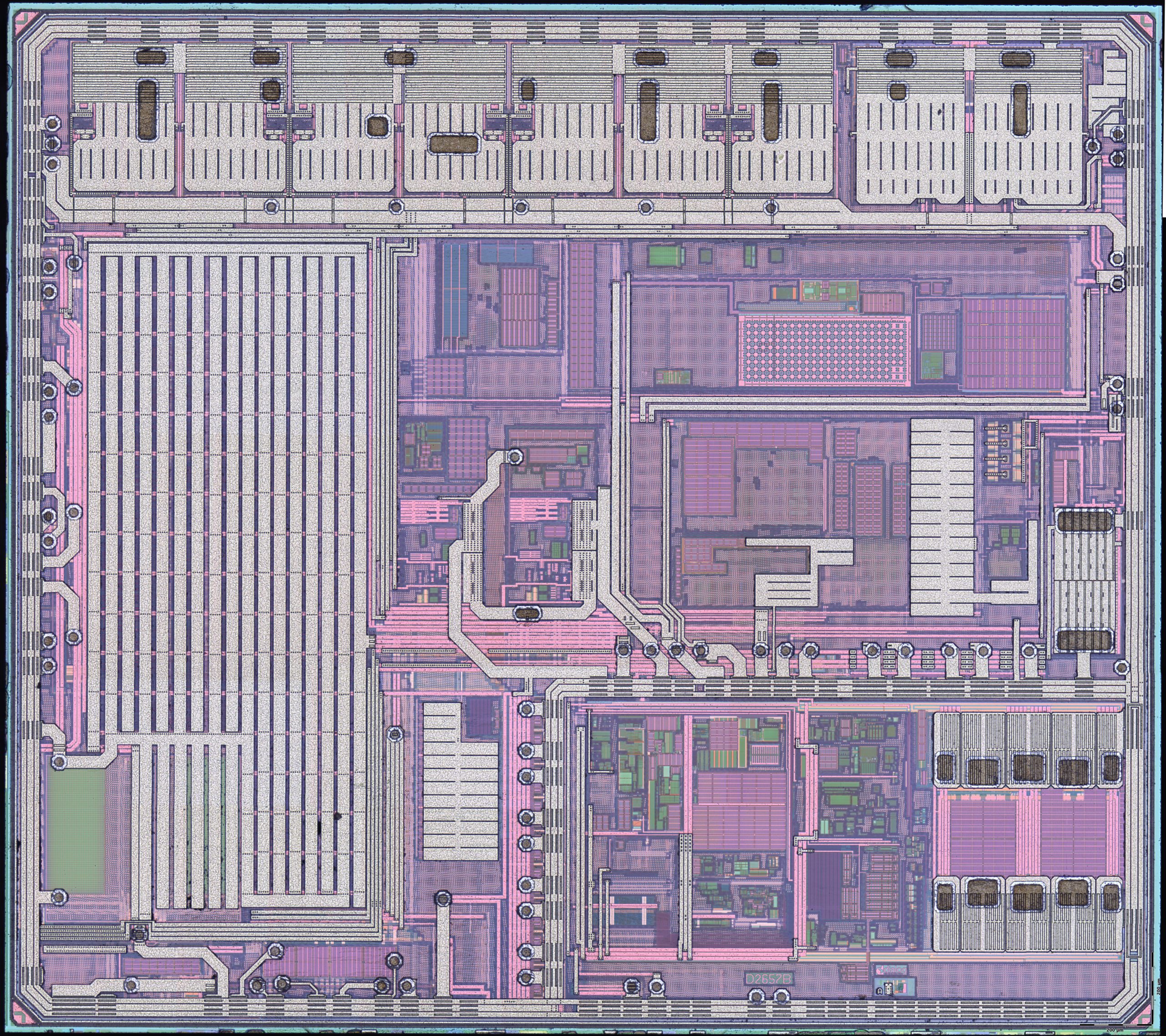
Reverse Engineering
"How it's made?" NanoPhysics B.V. reveals a device's construction, what components are inside and what materials are used.…
Read more
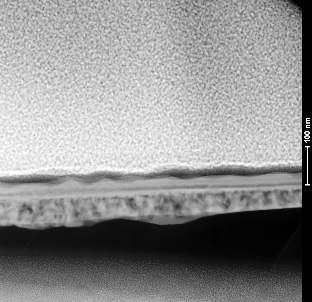
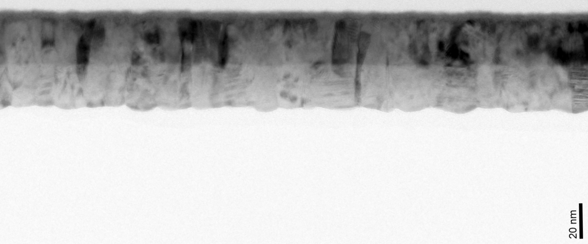
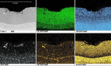
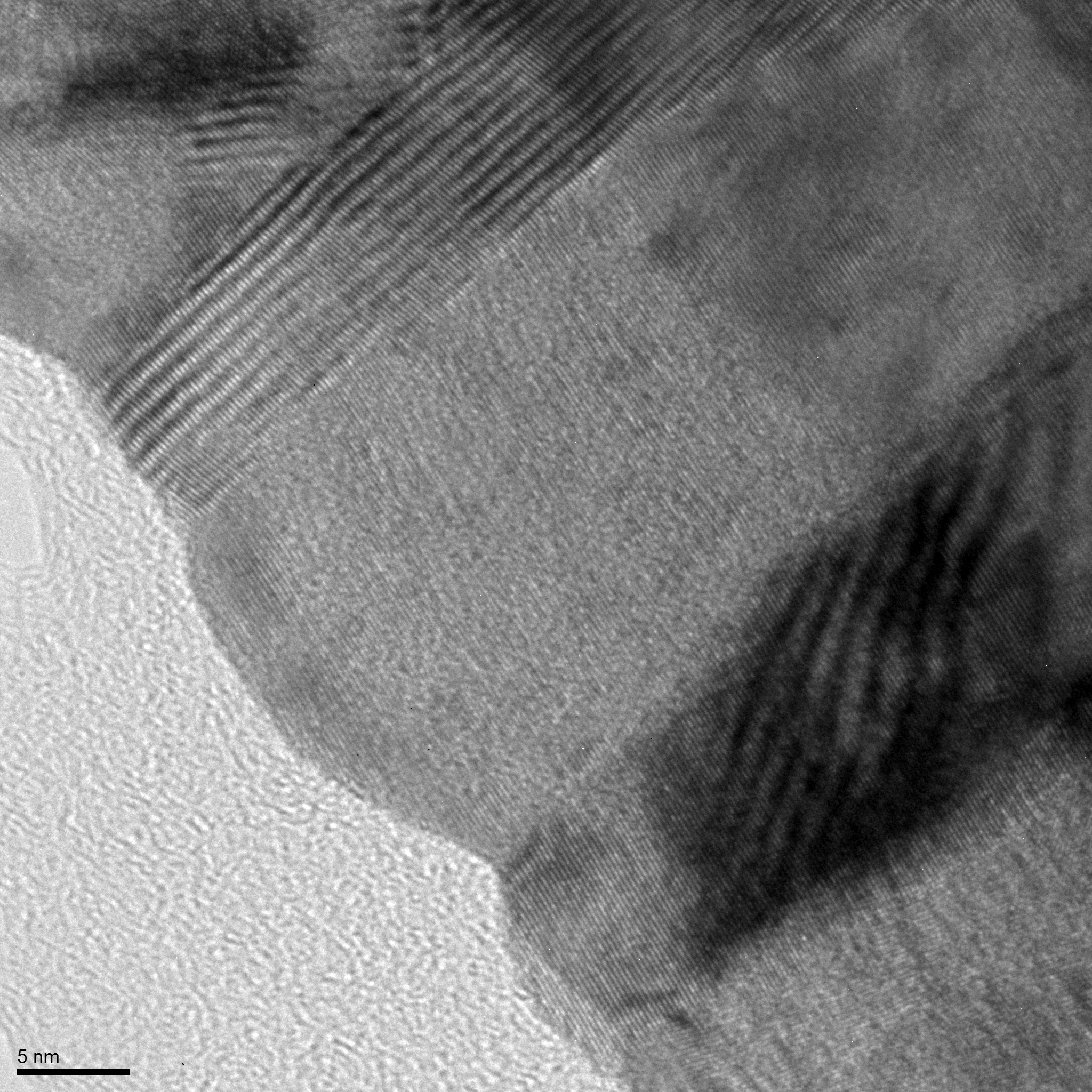
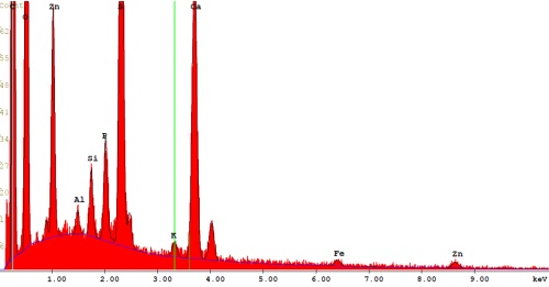
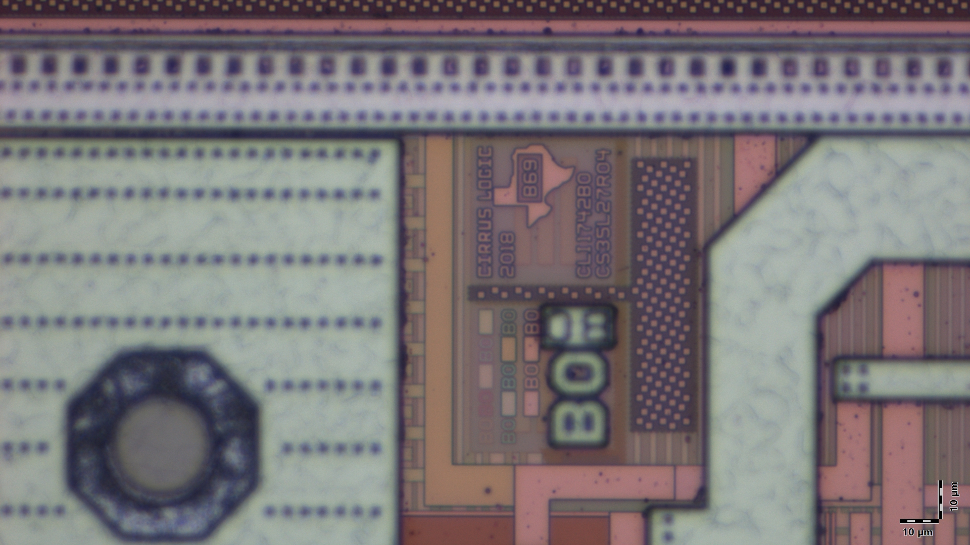
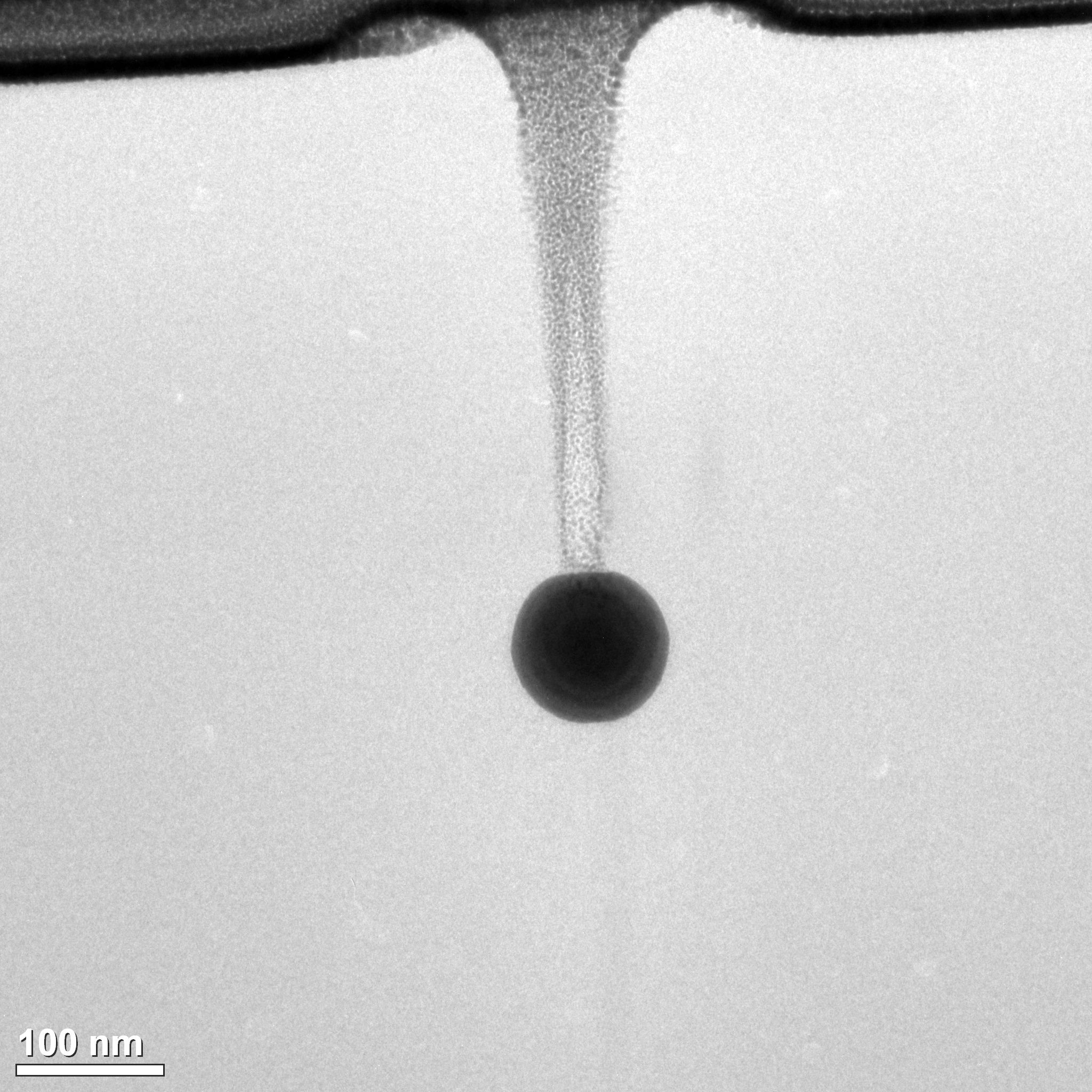
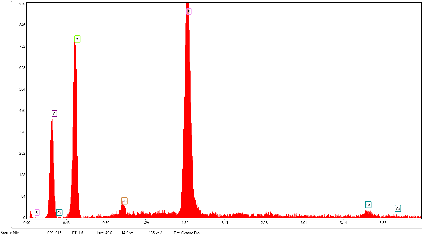
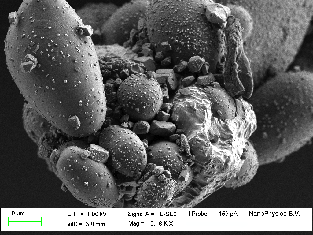
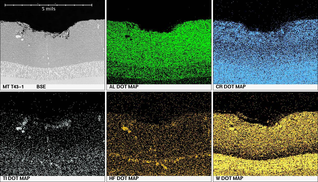
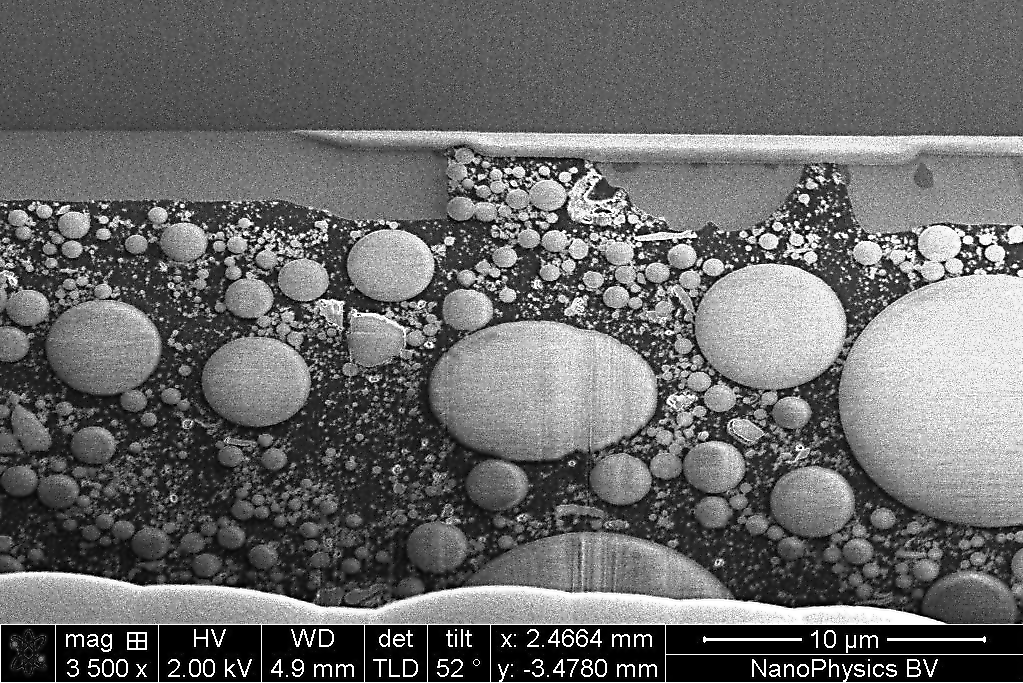
SEM-EDX
A powerful technique in Material Analysis is Scanning Electron Microscopy (SEM). Here a sample surface is scanned with a finely…
Read more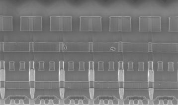
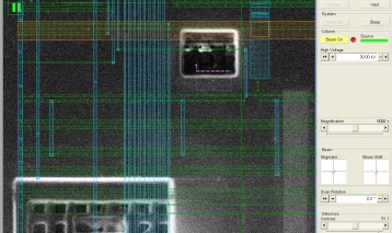
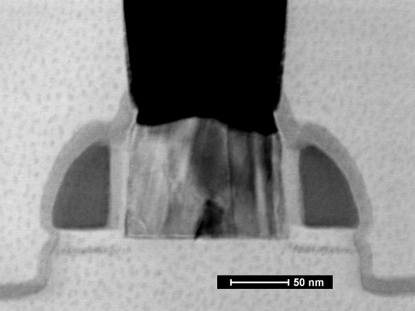
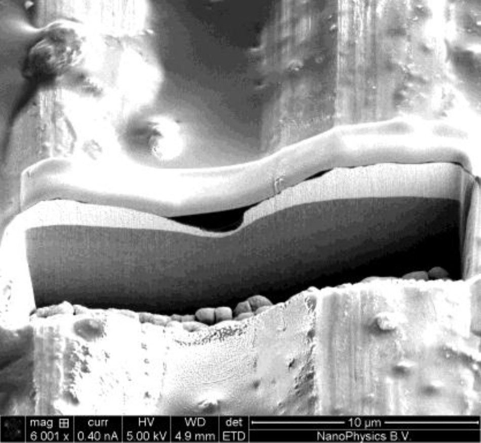
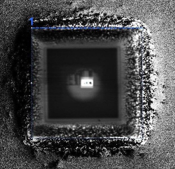
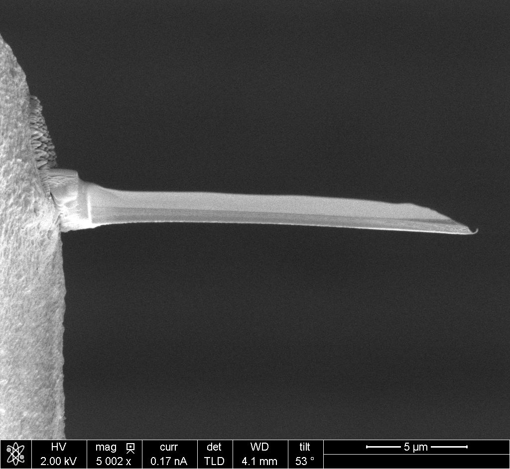
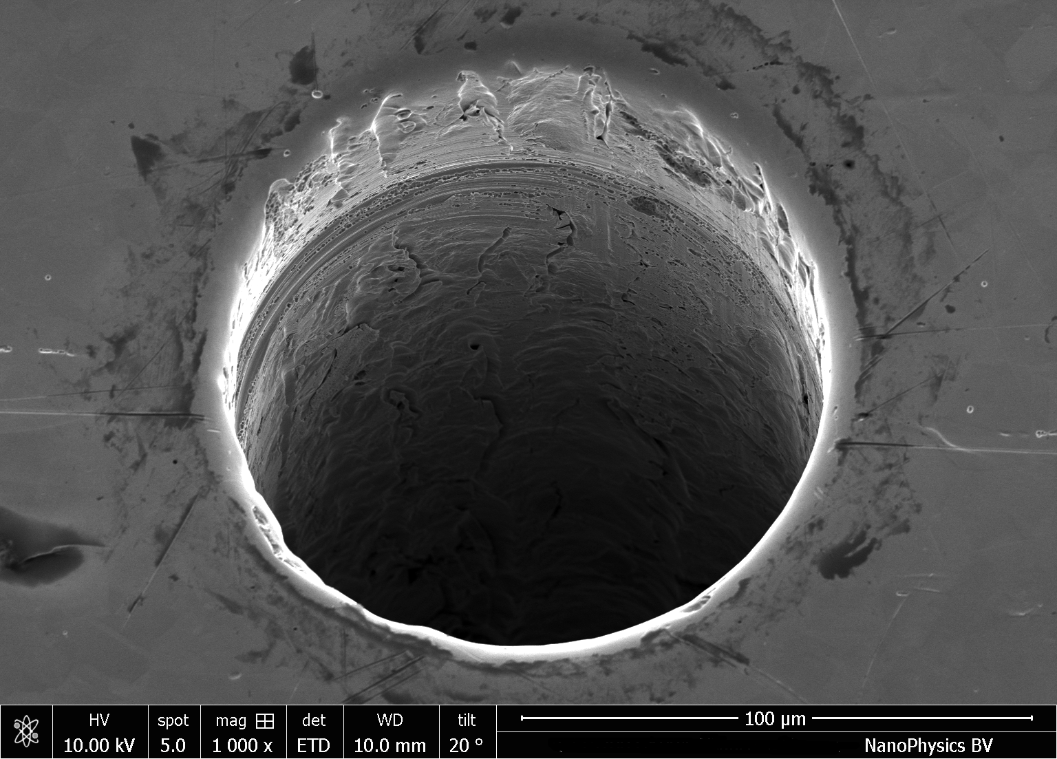
FIB cross sectioning
A Focused Ion Beam (FIB) system is a powerful tool that offers a wide range of applications in…
Read more