A Focused Ion Beam (FIB) system is a powerful tool that offers a wide range of applications in various fields. Its primary use lies in the realm of nanotechnology and materials science. With a FIB system, researchers and engineers can precisely etch, mill, and pattern materials at the nanoscale, enabling them to create intricate structures and modify material properties with exceptional precision. Additionally, FIB systems are crucial in semiconductor manufacturing, as they can be used for circuit editing, failure analysis, and device modification. Moreover, in the field of microscopy, FIB allows for cross-sectioning and imaging of materials, providing valuable insights into their internal structures. Furthermore, FIB systems play a vital role in sample preparation for transmission electron microscopy (TEM) analysis. Overall, the versatility and accuracy of FIB systems make them indispensable in advancing scientific research, electronics development, and nanofabrication technologies.
An example:
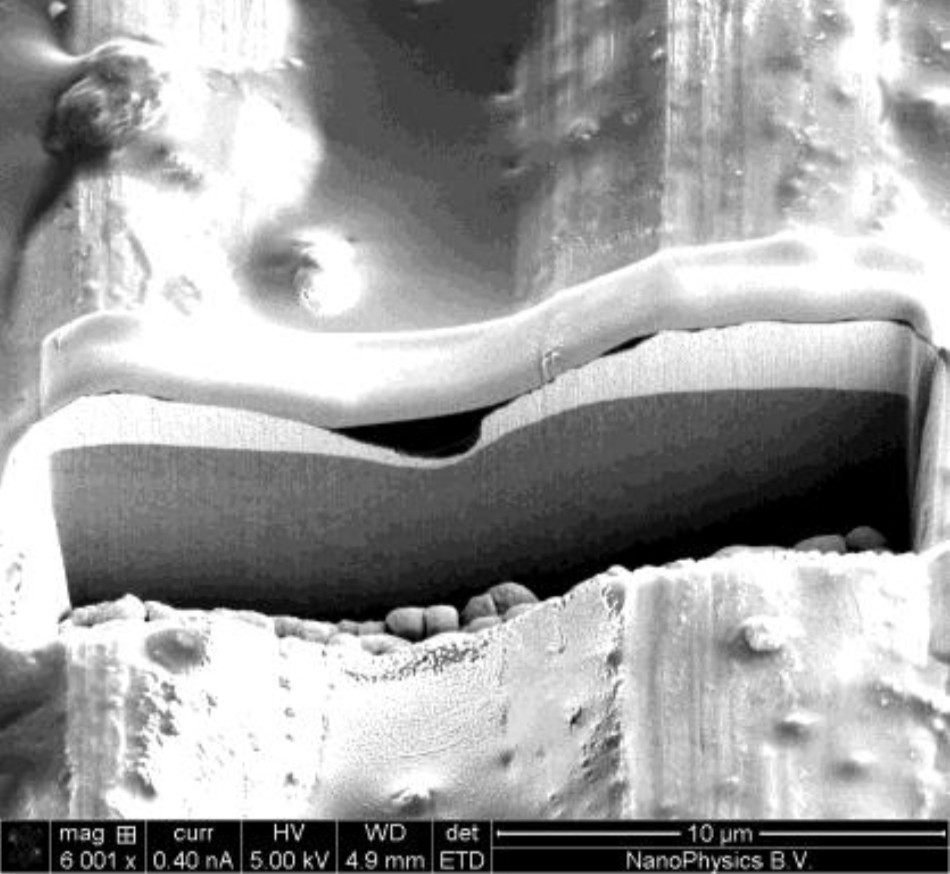
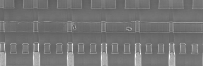
FIB cross-section showed interruption of plating
For an electrical connector, it is important that the gold plating is thick enough and has good wear- resistance over its lifetime. To get a good image of such plating a Focused Ion Beam (FIB) is used. A tiny hole is milled and the resulting polished surface is analyzed using an electron microscope. In most case this electron microscope and FIB are combined in a so called DualBeam system.
FIB cross section features:
- FIB-prepared sections are used extensively in SEM microscopy, where the FIB preparation, SEM imaging, and elemental analysis are done on the same DualBeam system.
- It is an ideal tool for examining products with small, difficult-to-access features, as found in the semiconductor industry and for sub-surface particle identification.
- NO mechanical stress is applied to your sample
- NO contaminants like grinding/polishing slurries are applied
- It is a good alternative for products that are difficult to mechanically polish, such as a soft polymers.
Some applications:
- Thin film coatings
- Plating thicknesses
- Elucidate a specific IC structure or Failure Analysis hotspot
- Metal stack cross sectioning to reveal al metal layers in a semiconductor device
- Reverse engineering (e.g., reveal proces node of IC)
- Reveal a particle or feature (like grain boundary or an inclusion)
In case you want us to review your case do not hesitate to contact us.
More Services: SEM-EDX, Chip Deprocessing, FIB cross sectioning, Competitor Analysis on chip, Semiconductor Patent Infringement analysis, FIB Circuit Edit, Failure Analysis, Reverse Engineering solutions