
A powerful technique in Material Analysis is Scanning Electron Microscopy (SEM). Here a sample surface is scanned with a finely focussed electron beam. The resulting electron bombardment leads to the emission of secondary electrons, backscattering of high energy primary electrons and creation of element specific X-rays. Several detectors are available in Electron Microscopy all with their advantages. SE detectors only collects low energy secondary electrons originate from the top nanometers of the sample. This give excellent surface topography images with very reasonable resolution.
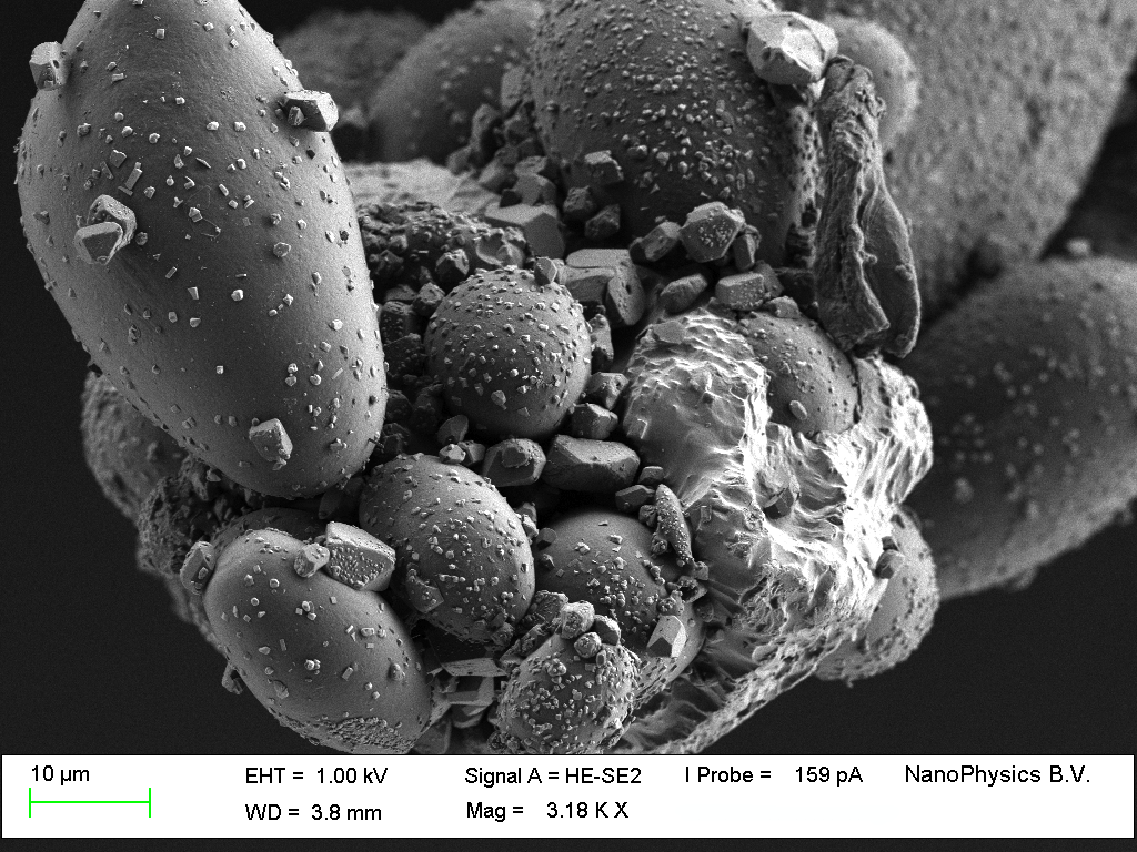
SE image of particle
Backscatter detector only collects primary electrons. These high energy electrons, on the other hand, is determined by the average atomic number of the sample material. The corresponding images clarify the distribution of different materials (Z-contrast images). This is perfect for layer determination, as each layer contains different element it is easily to distinguish. In Backscatter mode, the information depth is in the range of 1 µm. In other words you can obtain information till about 1 µm underneath the surface. One other detector we would highlight is the Inlens- or Through Lens Detector. This detector is placed in the electron column and is coaxial to the electron beam. The sample surface needs to be close to column for optimal performance. This detector is not recommended for surface topography but it does achieve the highest magnitudes possible.
A big advantage of SEM compared to optical microscopy besides high magnitudes is the depth of focus. With SEM a particular surface can be inspected using angled view while the surface is in focus throughout the whole image.
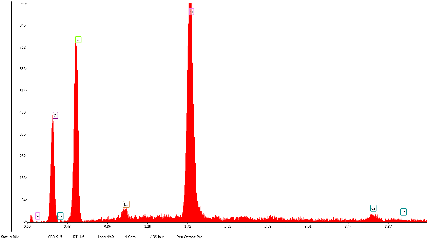
EDX elemental analysis
Energy Dispersive X-rays Spectroscopy (EDX or EDS) is an analytical capability were element specific radiation is used for chemical characterisation of the surface near volume. With the aid of proper detectors, the energy or the X-rays is determined. It can be coupled with several applications including Scanning Electron Microscopy (SEM), Transmission Electron Microscopy (TEM) and Scanning Transmission Electron Microscopy (STEM).
EDX, when combined with SEM, provides elemental analysis on areas as small as nanometers in diameter. The impact of the electron beam on the sample produces x-rays that are characteristic of the elements found on the sample. The measured intensities yield quantitative information on the element composition and distribution. The depth from where the X-rays originate depends on the material and the used primary electron beam energy. For typical primary energies of 10 to 20 keV it is in the µm range.
Samples for SEM and/or EDX need to be high vacuum compatible. However for some applications like moisturous or non-conductive samples Environmental SEM (ESEM) is also possible allowing chamber pressures up to 1 mbar.
Some applications:
- Identification of metals and materials
- Particle contamination identification and elimination
- Classification of materials
- Product and process failure and defect analysis
- Examination of surface morphology (including stereo imaging)
- Analysis and identification of surface and airborne contamination
- Powder morphology, particle size and analysis
- Cleaning problems and chemical etching
- Welding and joining technology quality evaluation and failure investigation
- Paint and coating failure and delamination investigation
- Identification and elimination of corrosion and oxidisation problems
- Contamination or stain investigation
- Structural analysis
- Reverse engineering of products and processes
Do not hesitate to contact us for information without obligation about our SEM service.
More Services: SEM-EDX, Chip Deprocessing, FIB cross sectioning, Patent Infringement analysis, Competitor Analysis, FIB Circuit Edit, Failure Analysis, Reverse Engineering
