According Moores law, every two years the amount of transistors on a chip is doubled. Through the years, the chip manufacturers are competing each other with the most recent technology available. This in practice means that it reflects to the dimension of the switching part of the transistor. This is called the gate and the length of it is called the process node. The smaller the process node, the more transistors are applicable to the chip and the more complex the used technology is. For companies or IDMs it is of interest to know which process node is used by the competitor for a competitive product or chip.
NanoPhysics has a reverse engineering service to deduce the technology node by using FIB cross sectioning or site specific TEM lamella preparation in a high density area of transistors. But first the samples has to be prepared either by planar lapping on the frontside or we can remove the complete silicon backside. For the imaging of such process node a High Resolution SEM is used.
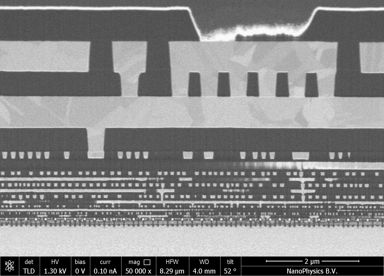
FIB cross section of TSMC 5NP process
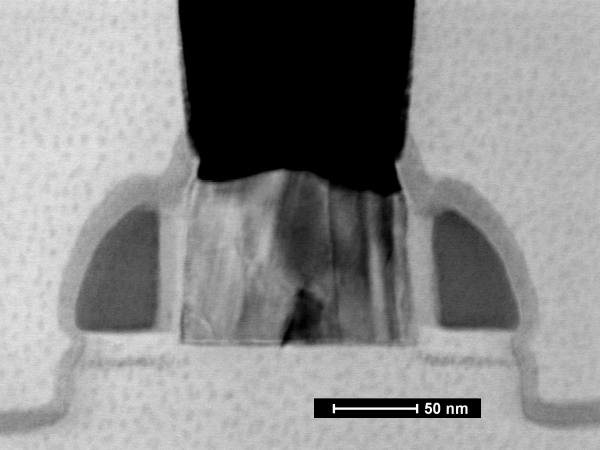
For even more details we advise to perform Transmission Electron Microscopy (TEM). In the figure in the left an example is given of such a TEM analysis. The result is the same, except that higher magnifications are possible and because of this more detail can be obtained with higher resolution.
